MODERN TECHNIQUES (ALD and PECVD) FOR THIN LAYER DEPOSITION FOR
NANOELECTRONICS APPLICATIONS
14 – 15 July, 2015
Sofia, Bulgaria
PROGRAMME
14 July 2015
| 10:00 – 10:10 | Openning by prof. Kostadinka Gesheva |
| 10:10 – 11:00 | Dimitre Dimitrov “Atomic layer deposition for photovoltaics” |
| 11:00 – 11:20 | Coffee-break |
| 11:20 – 12:10 | Peter Rafailov ”CVD processes for carbon nanotubes and graphene growth” |
| 12:10 – 13:00 | Jerome Leclercq ”Porous anodic alumina composite made with PECVD and ALD technology” |
| 13:00 – 14:00 | Lunch |
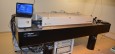
| 14:00 – 16:00 | Visit to the corresponding facilities at the Institute of Solid State Physics (ALD and PECVD) |
15 July 2015
| 10:30 – 11:20 | Hermine Stroescu ”Ellipsometry for films characterization: VASE ellipsometer M2000D” |
| 11:20 – 11:40 | Coffee-break |
| 11:40 – 12:30 | Peter Rafailov “Raman spectroscopy for characterization of carbon nanotubes and graphene” |
| 12:30 – 14:00 | Lunch |
 Saving...